Albert Einstein received the Nobel Prize in Physics for his famous theory of relativity if not for his work on the photoelectric effect, being the first to offer a theoretical explanation.
The photoelectric effect was discovered, as has often happened in history, by chance. In the late nineteenth century, Heinrich Hertz realized that the electric arc between two high voltage electrodes getting longer distances when illuminated with UV light to dark. Decades after Albert Einstein published a mathematical theory to explain this phenomenon which earned him the Nobel Prize in Physics.
The photoelectric effect is produced in certain materials by receiving light.
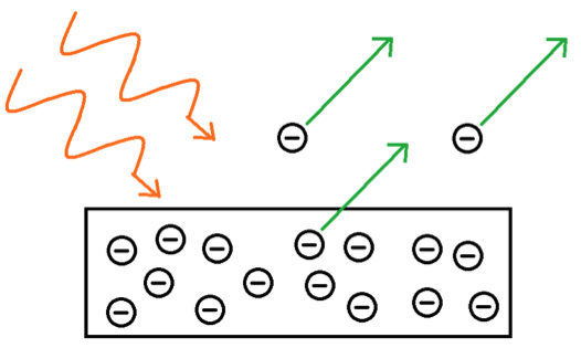
Thanks to the discovery of Hertz and the work of Einstein, solar PV has been able to de developed as we know it today, allowing the transformation of light from the sun into usable electrical energy.
The basic element of this transformation is the solar cell. Generally made of silicon, although other materials may be used, the solar cells can be wafer (manufactured by fine cuts on a solid block of silicon) or primers applied by deposition of material on a substrate. The first, based on crystalline silicon, provide high efficiency at a relatively higher cost, while the second, called Thin Layer technology or “thin film”, provides a cheaper alternative, but less efficiently.
Photoelectric effect due to the incidence of sunlight on certain appropriately treated semiconductor materials such as silicon or other materials, produces a potential difference (one positive and one negative) causing a DC.
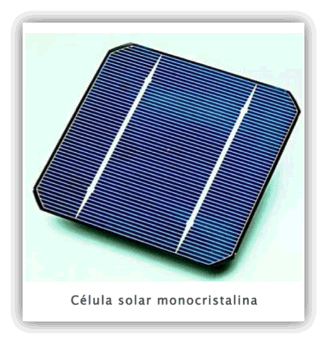
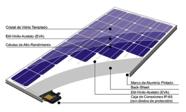
The solar cells are encapsulated in different layers of materials, as a “sandwich” to form modules (or panels) PV, a more manageable, interconnectable and protected from the weather unit.
The Solar Photovoltaic module is the main element of electricity generation from sunlight. Consists of:
- Photovoltaic cells or interconnected and encapsulated in different materials as a “sandwich”, as indicated previously in greater detail.
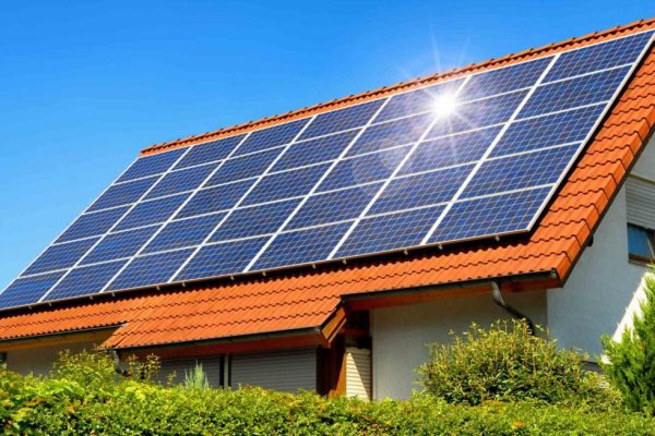
- Encapsulant and protective glass. First, the various encapsulating layers protect from weather and electrically isolated, and the glass allows the passage of light while protecting the cells against impact (hail, bumps, dirt, etc.). It is vital for module durability.
- The metal frame, whose mandate is to stiffen the assembly and facilitate mounting the module to a structure. It is not always present.
- Junction box or later. Facilitates waterproof connection pool of cells up to the positive and negative end cables, and hosts the bypass diodes; elements disconnected branches of cells to prevent electrical problems with partially shaded module.
- Cable connection. Usually, connectors for positive and negative, facilitating the interconnection between them in forming strings (strings of modules interconnected).
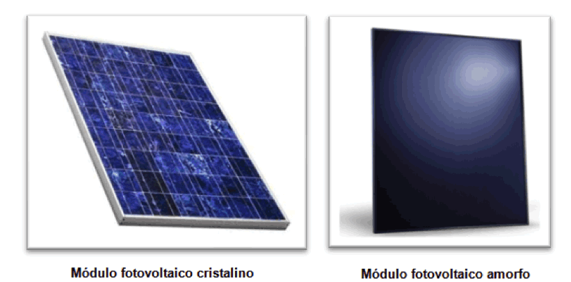
Two main types of modules are distinguished by cell technology used (although other technologies: CPV, organic and polymer cells, etc.):
- Crystalline photovoltaic modules: either monocrystalline or polycrystalline in its version; if crystalline silicon is used as the base material of manufacture. This is the most used, between 80 and 90% of global modules manufactured using silicon technology. In the single crystal case, the cells that form the module are comprised of single crystal silicon, polycrystalline while the cells are formed by multiple crystals in different orientations. The process of obtaining monocrystalline cells is longer and more complex, making them more expensive, but in return, greater production efficiencies are obtained electricity.
- Amorphous photovoltaic modules: include diverse technologies with the use of other materials such as a-SI, CdTe, CIGis, CIS, etc. Used are less on their lower efficiency, which implies larger surface for tºhe same installed power compared to that required in the monocrystalline and polycrystalline technology; which is why we always used with a fixed structure. Lose less performance at high temperature, which are used in areas of high irradiance.

Pol Parareda Farriol es ingeniero industrial y MBA, con más de 15 años de experiencia internacional en el sector de la energía solar fotovoltaica y las energías renovables. Actualmente Director en Tienda Solar, trabaja en el desarrollo y gestión de soluciones de autoconsumo, sistemas fotovoltaicos y almacenamiento con baterías para el mercado residencial y profesional.
A lo largo de su carrera ha ocupado puestos de responsabilidad en empresas líderes del sector como Weidmüller, SunPower, Sunco Capital y Hilti, desempeñando funciones en ingeniería, desarrollo de producto, operaciones, O&M, gestión comercial y dirección estratégica de proyectos solares, tanto a pequeña escala como en grandes plantas fotovoltaicas internacionales.
Ha liderado proyectos y equipos en Europa, Latinoamérica y Asia, participando en el desarrollo de más de cientos de MW en proyectos solares, negociación de PPAs, estrategias EPC y optimización de sistemas fotovoltaicos. Además, ha sido docente de energía solar fotovoltaica en programas de máster en energías renovables en instituciones como la Universidad Carlos III de Madrid


